How to use QSPI flash memory with EK-RA6M4 board
By Toni Akkala, 23rd of August, 2022
Overview
In this blog, we will show you how to implement a CMSIS compatible QSPI flash memory driver for a Macronix MX25L25645G flash memory when using a Renesas EK-RA6M4 board.
Hardware
The Renesas EK-RA6M4 board includes the Macronix 32 MB Quad-Serial Peripheral Interface (QSPI) NOR flash memory. The idea behind Quad-SPI is to use four wires to transfer 4 bits in parallel to gain higher transfer rate. The flash memory is capable of using SI, SO, Write Protect (WP) and RESET pins as Serial Input/Output (SIO) pins when used in four I/O read mode. The following figure from the Macronix datasheet illustrates the idea and the benefit of using those extra wires with Write Enable command using SPI and Quad Peripheral Interface (QPI) mode.

Figure: Benefit of using Quad-SPI with QPI mode
The flash memory can be used either in serial mode 0 (CPOL=0, CPHA=0) or serial mode 3 (CPOL=1, CPHA=1). When the flash memory is not selected Chip Select (CS) being in high state, it is in standby mode. To exit from the standby mode, a valid command must be written to the flash memory. Then it will remain in active state until the next CS rising edge. After power on, the EK-RA6M4 board flash memory has Execute-In-Place (XIP) enabled which means that one would be able to run the code directly from the flash memory without copying the code to the RAM first.
FSP
Renesas Flexible Software Package (FSP) supports QSPI flash memory with r_qspi module. Renesas RA Smart configurator can be used to configure several options for this module, like used SPI protocol, number of address bytes used or the selected read mode. The clock source for the QSPI module is PCLKA, running at 100 MHz. The following figure shows the clock configuration used in this project.
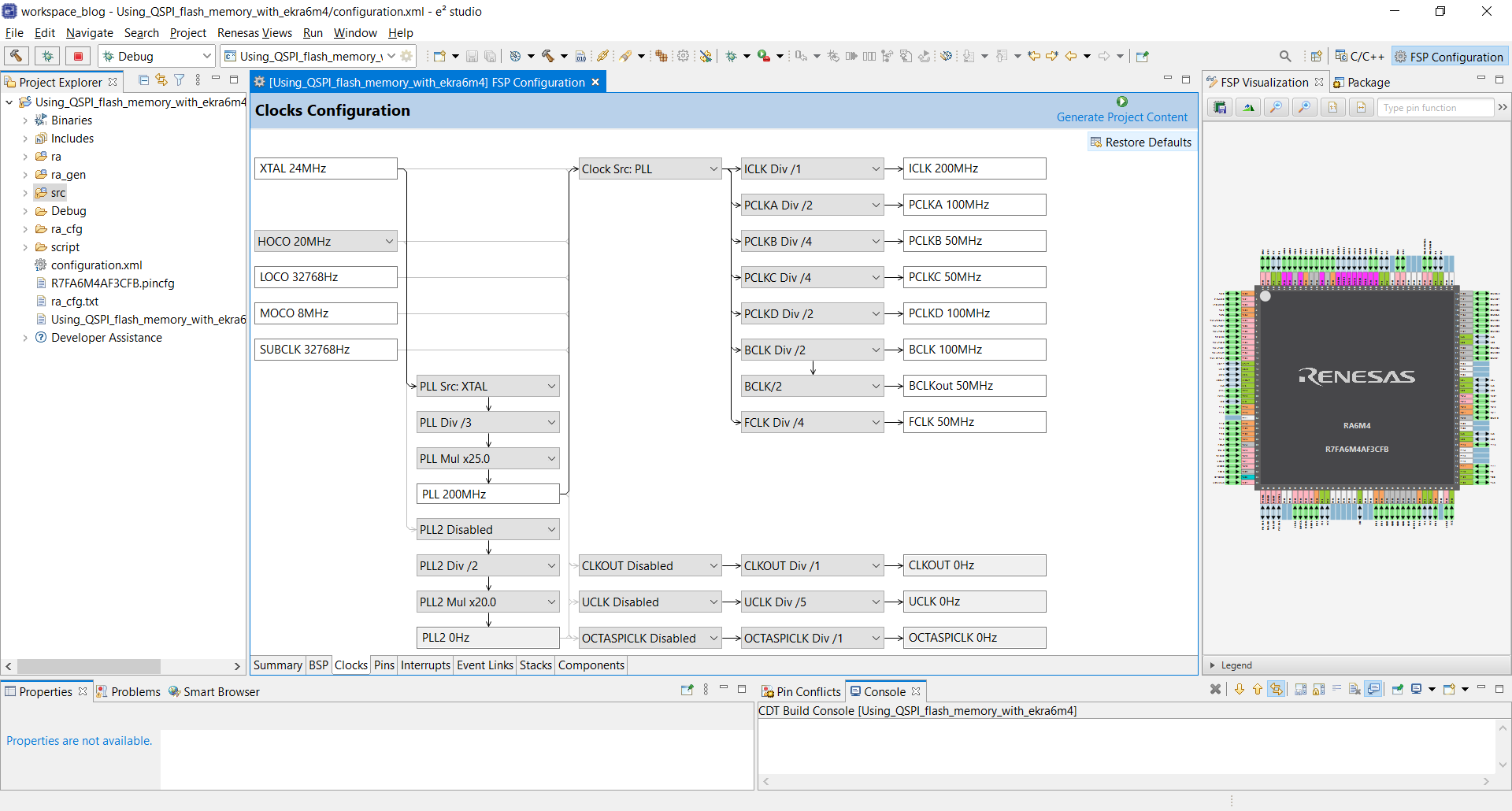
Figure: FSP clock configuration
There is also a divider setting QSPKCLK Divisor used to divide the PCLK to get QSPCLK. With the default amount of dummy clock cycles, the maximum clock frequency for the flash memory is 80 MHz in the Quad I/O fast read mode. With the divisor value 2, we will get 50 MHz clock for the QSPI which means that maximum clock frequency will not be exceeded.
Once the driver has been added to a FSP stack and configured, user can call R_QSPI_Open(), after which QSPI flash memory contents are memory mapped at 0x60000000 address for reading. From the following figure we can see the FSP stack and the variable name used in code for the QSPI driver control (g_qspi0). Once everything is set, you can just click Generate project content to create HAL driver for you with the chosen configuration. e2 studio will include generated files to the project automatically.
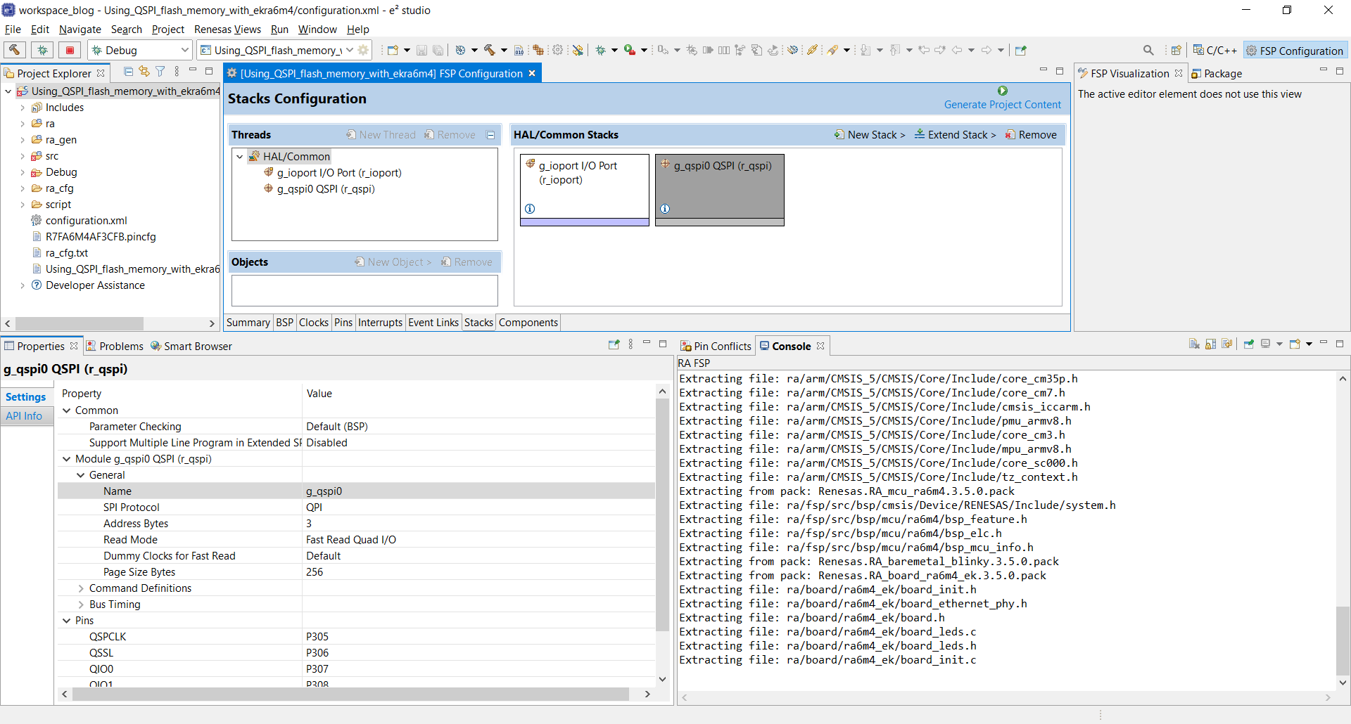
Figure: FSP stack configuration
About SPI protocol selection
QPI read mode must be enabled with a separate command. These commands are written to the flash memory by using R_QSPI_DirectWrite function. EQIO command enables QPI mode and it must be disabled with a RSTQIO command. FSP function R_QSPI_SpiProtocolSet() can be used to configure microcontroller (MCU) to the extended SPI or QPI mode. The user must first write these commands to the flash memory before switching the MCU mode, otherwise the flash memory will be in different mode than the MCU. Also after reset, you might not know in which state the flash memory is in. It might be safe to switch MCU to the QPI mode, then execute RSTQIO command and then switch MCU back to extended SPI mode to make sure that both the MCU and the flash memory are in extended SPI mode during configuration. This is the approach I will use in this implementation.
CMSIS Flash memory driver
Common Microcontroller Software Interface Standard (CMSIS) specifies an API which consists of several different peripheral drivers, including the flash memory driver. When underlying HAL driver needs to be changed because of hardware change for example, application code does not have to be modified as the CMSIS API does not change. Only the driver implementing CMSIS driver functionalities must be created to support the new hardware. I will use this interface with an spi_flash_api_t API to link my application to the Renesas QSPI HAL driver.
Implementation
I downloaded the CMSIS driver headers and driver template files from a Arm software github repository. I added the template files to the e2 studio project I created for the FSP configuration and renamed those files for my project. From the headers, I included Driver_Common.h and Driver_Flash.h files to my project. From the FSP, I included hal_data.h. After this, I was able to build the project without errors.
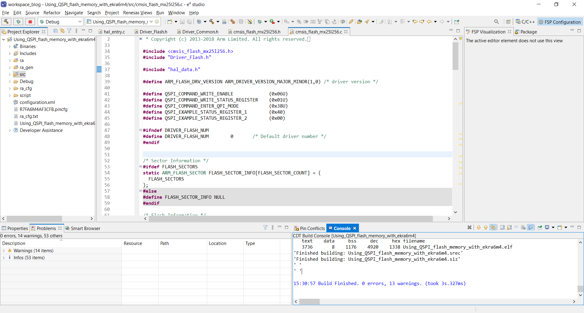
Figure: Successful build
After successful build I started to implement those driver functions in the template. Here is the code for the interesting functions excluding some of the content from the file:
...
#include "Driver_Flash.h"
#include "cmsis_flash_mx25l256.h"
#include "hal_data.h"
...
#define QSPI_COMMAND_WRITE_STATUS_REGISTER (0x01U)
#define QSPI_COMMAND_READ_STATUS_REGISTER (0x05U)
#define QSPI_COMMAND_ENTER_QPI_MODE (0x35U)
#define QSPI_COMMAND_EXIT_QPI_MODE (0xF5U)
#define QSPI_COMMAND_READ_ID_SPI_MODE (0x9FU)
#define QSPI_COMMAND_READ_ID_QPI_MODE (0xAFU)
...
/*
* Pointer to SPI flash API.
*/
static const spi_flash_api_t *memory_api_p = &g_qspi_on_spi_flash;
/*
* Pointer to SPI flash control structure.
*/
static spi_flash_ctrl_t *memory_control_p = &g_qspi0_ctrl;
/*
* Pointer to SPI flash configuration structure.
*/
static const spi_flash_cfg_t *memory_config_p = &g_qspi0_cfg;
/*
* Function to read status register until write is not in progress
*
* @return True if successful, false otherwise
*/
static bool driver_wait_while_wip(void)
{
spi_flash_status_t status;
do {
if (FSP_SUCCESS != memory_api_p->statusGet(memory_control_p, &status)) {
return false;
}
} while (true == status.write_in_progress);
return true;
}
/*
* Set extended SPI Mode for flash device and MCU
*
* @return True if successful
*/
static bool driver_set_spi_mode(void)
{
fsp_err_t err = FSP_SUCCESS;
// Switch MCU to QPI mode and issue commands to memory to exit from QPI
err = memory_api_p->spiProtocolSet(memory_control_p, SPI_FLASH_PROTOCOL_QPI);
if (FSP_SUCCESS != err) {
return false;
}
// Remove write protection
err = memory_api_p->directWrite(memory_control_p, &(memory_config_p->write_enable_command), 1, false);
if (FSP_SUCCESS != err) {
return false;
}
// and exit from QPI to extended SPI mode
uint8_t data_spi_en = QSPI_COMMAND_EXIT_QPI_MODE;
err = memory_api_p->directWrite(memory_control_p, &data_spi_en, 1, false);
if (FSP_SUCCESS != err) {
return false;
}
// Switch MCU to SPI mode
err = memory_api_p->spiProtocolSet(memory_control_p, SPI_FLASH_PROTOCOL_EXTENDED_SPI);
if (FSP_SUCCESS != err) {
return false;
}
return true;
}
/*
* Set QPI Mode in flash device and MCU
*
* @return True if successful
*/
static bool driver_set_qpi_mode(void)
{
fsp_err_t err = FSP_SUCCESS;
// Remove write protection
err = memory_api_p->directWrite(memory_control_p, &(memory_config_p->write_enable_command), 1, false);
if (FSP_SUCCESS != err) {
return false;
}
// send QPI mode enable command to the flash device
uint8_t data_qpi_en = QSPI_COMMAND_ENTER_QPI_MODE;
err = memory_api_p->directWrite(memory_control_p, &data_qpi_en, 1, false);
if (FSP_SUCCESS != err) {
return false;
}
// and then change MCU protocol, now both are in QPI mode
err = memory_api_p->spiProtocolSet(memory_control_p, SPI_FLASH_PROTOCOL_QPI);
if (FSP_SUCCESS != err) {
return false;
}
return true;
}
/*
* Write command to QSPI memory and read the response without
* asserting CS in between.
*
* @param command QSPI memory command.
* @param buffer Buffer for data to be read.
* @param buffer_size Number of bytes to read.
*
* @return True if successful, false otherwise
*/
static bool driver_write_command_read_response(const uint8_t command, uint8_t *buffer, const size_t buffer_size)
{
if (FSP_SUCCESS != memory_api_p->directWrite(memory_control_p, &command, 1, true)) {
return false;
}
if (FSP_SUCCESS != memory_api_p->directRead(memory_control_p, buffer, buffer_size)) {
return false;
}
return true;
}
/*
* Initialize flash memory to the selected mode.
*
* @return True for success, false otherwise
*/
static bool driver_initialize(void)
{
fsp_err_t err;
uint8_t data[4];
err = memory_api_p->open(memory_control_p, memory_config_p);
if (FSP_SUCCESS != err) {
return false;
}
// Set extended SPI mode
if (false == driver_set_spi_mode()) {
return false;
}
// Remove write protection
err = memory_api_p->directWrite(memory_control_p, &(memory_config_p->write_enable_command), 1, false);
if (FSP_SUCCESS != err) {
return false;
}
// Configure status and configuration register
data[0] = QSPI_COMMAND_WRITE_STATUS_REGISTER;
data[1] = 0x40; // Quad Enable bit set
data[2] = 0x00;
err = memory_api_p->directWrite(memory_control_p, &data[0], 3, false);
if (FSP_SUCCESS != err) {
return false;
}
// Wait for status register to update
if (false == driver_wait_while_wip()) {
return false;
}
// Read status register
data[0] = QSPI_COMMAND_READ_STATUS_REGISTER;
err = memory_api_p->directWrite(memory_control_p, &data[0], 1, true);
if (FSP_SUCCESS != err) {
return false;
}
err = memory_api_p->directRead(memory_control_p, &data[0], 1);
if (FSP_SUCCESS != err) {
return false;
}
if (data[0] != 0x40)
return false;
// Read device ID (SPI)
uint8_t command = QSPI_COMMAND_READ_ID_SPI_MODE;
if (memory_config_p->spi_protocol == SPI_FLASH_PROTOCOL_QPI) {
// enable QPI mode
if (false == driver_set_qpi_mode()) {
return false;
}
// Read device ID (QPID)
command = QSPI_COMMAND_READ_ID_QPI_MODE;
}
if (false == driver_write_command_read_response(command, data, 3)) {
return false;
}
// Check manufacturer ID values, these are from MX25L25645G datasheet
if (data[0] != 0xC2)
return false;
if (data[1] != 0x20)
return false;
if (data[2] != 0x19)
return false;
return true;
}
/**
\fn int32_t ARM_Flash_Initialize (ARM_Flash_SignalEvent_t cb_event)
\brief Initialize the Flash Interface.
\param[in] cb_event Pointer to \ref ARM_Flash_SignalEvent
\return \ref execution_status
*/
static int32_t ARM_Flash_Initialize(ARM_Flash_SignalEvent_t cb_event)
{
(void)cb_event;
return driver_initialize() ? ARM_DRIVER_OK : ARM_DRIVER_ERROR;
}
/**
\fn int32_t ARM_Flash_Uninitialize (void)
\brief De-initialize the Flash Interface.
\return \ref execution_status
*/
static int32_t ARM_Flash_Uninitialize(void)
{
fsp_err_t err = memory_api_p->close(memory_control_p);
if (FSP_SUCCESS != err) {
return ARM_DRIVER_ERROR;
}
return ARM_DRIVER_OK;
}
/**
\fn int32_t ARM_Flash_ReadData (uint32_t addr, void *data, uint32_t cnt)
\brief Read data from Flash.
\param[in] addr Data address.
\param[out] data Pointer to a buffer storing the data read from Flash.
\param[in] cnt Number of data items to read.
\return number of data items read or \ref execution_status
*/
static int32_t ARM_Flash_ReadData(uint32_t addr, void *data, uint32_t cnt)
{
memcpy(data, (void*)(QSPI_DEVICE_START_ADDRESS + addr), cnt);
return cnt > INT32_MAX ? INT32_MAX : (int32_t)cnt;
}
/**
\fn int32_t ARM_Flash_ProgramData (uint32_t addr, const void *data, uint32_t cnt)
\brief Program data to Flash.
\param[in] addr Data address.
\param[in] data Pointer to a buffer containing the data to be programmed to Flash.
\param[in] cnt Number of data items to program.
\return number of data items programmed or \ref execution_status
*/
static int32_t ARM_Flash_ProgramData(uint32_t addr, const void *data, uint32_t cnt)
{
uint32_t bytes_written = 0;
while (bytes_written < cnt) {
uint32_t data_size = FLASH_PAGE_SIZE;
uint32_t bytes_left = (cnt - bytes_written);
if (data_size > bytes_left) {
data_size = bytes_left;
}
uint8_t *address_p = (uint8_t*)(QSPI_DEVICE_START_ADDRESS + addr + bytes_written);
uint8_t *data_p = ((uint8_t*)data + bytes_written);
fsp_err_t err = memory_api_p->write(memory_control_p, data_p, address_p, data_size);
if (FSP_SUCCESS != err) {
return ARM_DRIVER_ERROR;
}
if (false == driver_wait_while_wip()) {
return ARM_DRIVER_ERROR;
}
bytes_written += data_size;
}
return ARM_DRIVER_OK;
}
/**
\fn int32_t ARM_Flash_EraseSector (uint32_t addr)
\brief Erase Flash Sector.
\param[in] addr Sector address
\return \ref execution_status
*/
static int32_t ARM_Flash_EraseSector(uint32_t addr)
{
// Parameter error if address is not at the sector boundary
if (addr % FLASH_SECTOR_SIZE != 0) {
return ARM_DRIVER_ERROR_PARAMETER;
}
// erase one sector starting from given address
fsp_err_t err = memory_api_p->erase(memory_control_p, (uint8_t*)addr, FLASH_SECTOR_SIZE);
if (FSP_SUCCESS != err) {
return ARM_DRIVER_ERROR;
}
if (false == driver_wait_while_wip()) {
return ARM_DRIVER_ERROR;
}
return ARM_DRIVER_OK;
}
/**
\fn int32_t ARM_Flash_EraseChip (void)
\brief Erase complete Flash.
Optional function for faster full chip erase.
\return \ref execution_status
*/
static int32_t ARM_Flash_EraseChip (void)
{
return ARM_Flash_EraseSector(SPI_FLASH_ERASE_SIZE_CHIP_ERASE);
}
...
ARM_DRIVER_FLASH flash_driver = {
.GetVersion = ARM_Flash_GetVersion,
.GetCapabilities = ARM_Flash_GetCapabilities,
.Initialize = ARM_Flash_Initialize,
.Uninitialize = ARM_Flash_Uninitialize,
.PowerControl = ARM_Flash_PowerControl,
.ReadData = ARM_Flash_ReadData,
.ProgramData = ARM_Flash_ProgramData,
.EraseSector = ARM_Flash_EraseSector,
.EraseChip = ARM_Flash_EraseChip,
.GetStatus = ARM_Flash_GetStatus,
.GetInfo = ARM_Flash_GetInfo
};
Testing
To run some happy path tests for the implementation, I added this test code to the hal_entry function:
// Test for the external flash memory
uint8_t write_buffer[FLASH_SECTOR_SIZE];
uint8_t read_buffer[FLASH_SECTOR_SIZE];
uint32_t address = FLASH_SECTOR_SIZE * 2;
uint32_t size = (FLASH_PAGE_SIZE + 10);
// Initialize external flash memory
flash_driver.Initialize(NULL);
// erase the first sector, read the data and compare to erased value
flash_driver.EraseSector(FLASH_SECTOR_SIZE * 0);
flash_driver.ReadData(0, read_buffer, FLASH_SECTOR_SIZE);
for (uint32_t i = 0; i < FLASH_SECTOR_SIZE; i++) {
assert(read_buffer[i] == FLASH_ERASED_VALUE);
read_buffer[i] = 0;
}
// repeat for the next sector
flash_driver.EraseSector(FLASH_SECTOR_SIZE * 1);
flash_driver.ReadData(FLASH_SECTOR_SIZE, read_buffer, FLASH_SECTOR_SIZE);
for (uint32_t i = 0; i < FLASH_SECTOR_SIZE; i++) {
assert(read_buffer[i] == FLASH_ERASED_VALUE);
read_buffer[i] = 0;
}
// Write data to the second sector
for (uint32_t i = 0; i < FLASH_SECTOR_SIZE; i++) {
// wraps around after 255
write_buffer[i] = ((i+1) % 256);
}
flash_driver.ProgramData(FLASH_SECTOR_SIZE, write_buffer, FLASH_SECTOR_SIZE);
// The first sector should still contain erased values
flash_driver.ReadData(0, read_buffer, FLASH_SECTOR_SIZE);
for (uint32_t i = 0; i < FLASH_SECTOR_SIZE; i++) {
assert(read_buffer[i] == FLASH_ERASED_VALUE);
read_buffer[i] = 0;
}
// and the second sector should contain written values
flash_driver.ReadData(FLASH_SECTOR_SIZE, read_buffer, FLASH_SECTOR_SIZE);
for (uint32_t i = 0; i < FLASH_SECTOR_SIZE; i++) {
assert(read_buffer[i] == ((i+1) % 256));
}
flash_driver.EraseSector(address);
flash_driver.ProgramData(address, write_buffer, size);
flash_driver.ProgramData(address + size, write_buffer + size, FLASH_SECTOR_SIZE - size);
flash_driver.ReadData(address, read_buffer, FLASH_PAGE_SIZE);
for (uint32_t i = 0; i < FLASH_SECTOR_SIZE; i++) {
assert(read_buffer[i] == ((i+1) % 256));
}
Now I can build the code and run my tests to check that the data will be programmed to the flash memory correctly using the QPI mode.
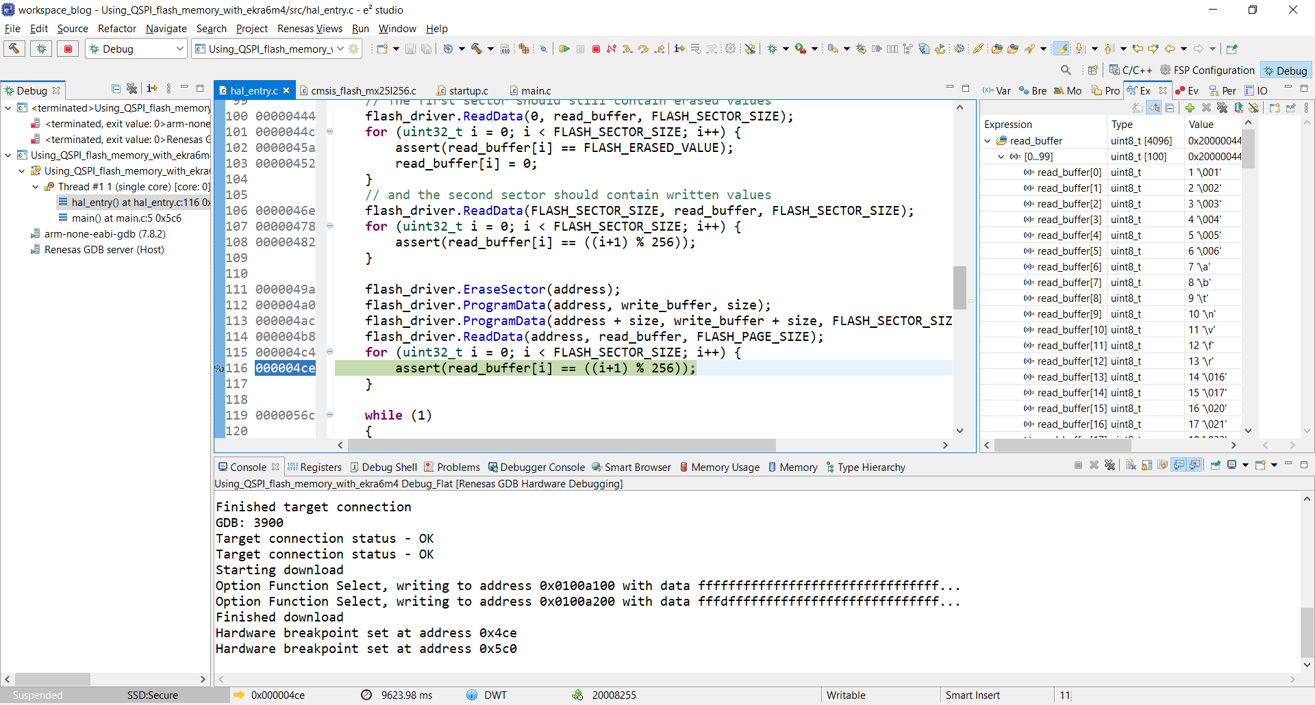
Figure: Debugging the code
Conclusion
As we can see, with the help of FSP, it is quite trivial to start using the flash memory with the CMSIS interface. QPI mode minimizes the clock cycles needed to transfer the data with the cost of circuit board size as you need to route more wires. Anyway, I would like to wrap this driver to the middleware filesystem layer some day.
References
